Compute#AI chips#Model training
Tesla lays out SI accelerator roadmap, with SI6 claimed at 80x HW4 compute
Tesla's November 6 slides lay out the SI roadmap: SI6 claimed at 80x HW4 compute for 2029-2030; Dojo D3 returns with chiplets plus stacked HBM for space.
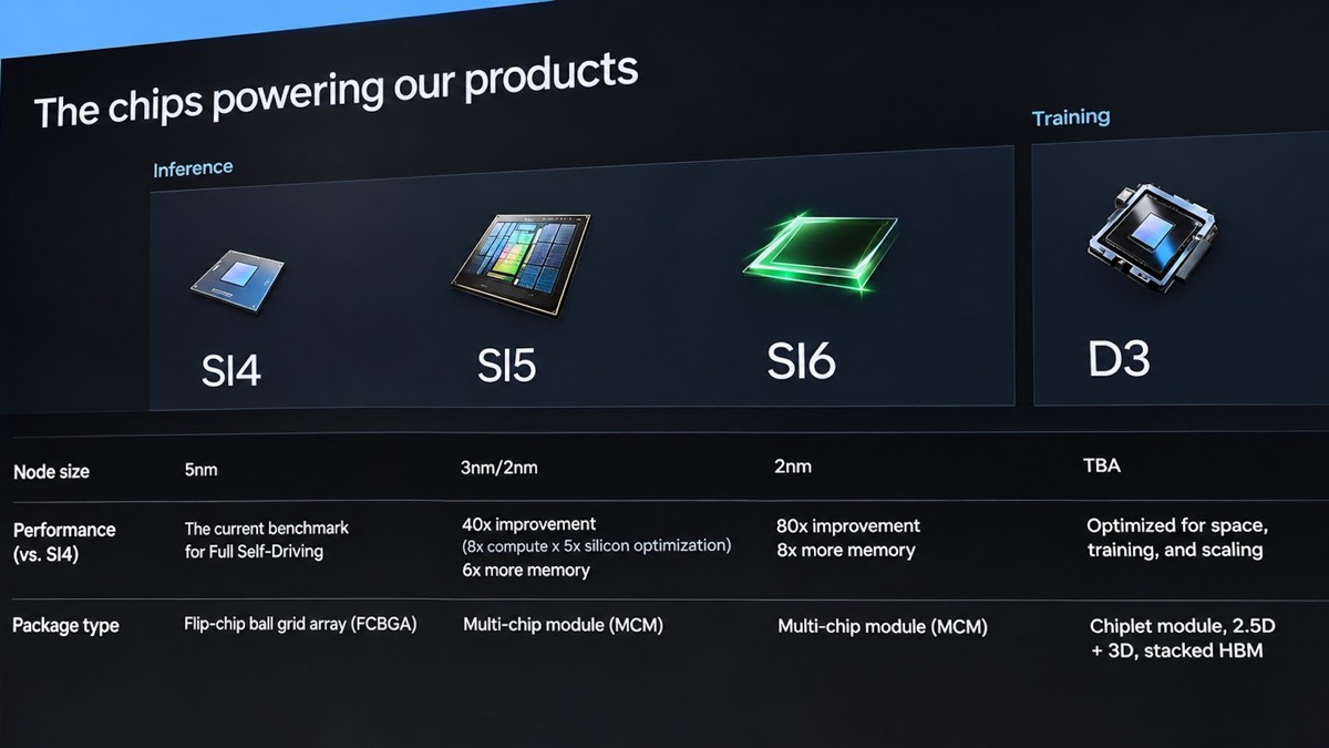
Tesla’s accelerator roadmap leaked into the open on November 6 as presentation slides photographed and published by Tom’s Hardware: the inference line runs from the current HW4 (relabeled SI4) through SI5, claimed at 40x SI4’s performance and nearing production, to SI6, claimed at 80x with a 2029-2030 arrival. The training chip Dojo D3 — left for dead when the wafer-scale project was cancelled in August 2025 — is back on the chart with a chiplet design and stacked HBM, its purpose line reading “optimized for space, training, and scaling.” Every multiple on that slide is Tesla’s own claim; Mezha and TipRanks picked it up the same day. None of the numbers has been measured by anyone outside the company.
Key points
- The slides relabel HW4/AI4 as SI4; SI5 is claimed at 40x (an 8x compute gain times 5x silicon optimization) with 96 GB of memory and 250-800 W power, marked “nearing production”; SI6 is claimed at 80x with 144 GB, a 2nm-class process and a 2029-2030 timeline
- Dojo D3 abandons D1’s wafer-scale SRAM architecture for chiplets with 2.5D/3D packaging and stacked HBM, targeting space, training and scaling — with no specs, process node or date disclosed
- The slide lists SI4’s process as 5nm; Tom’s Hardware notes that contradicts the known Samsung 7nm-class node — read this roadmap with a checker’s eye
Background
Tesla’s in-house chips have so far served exactly one customer: the car. HW3 was the 2019-era 14nm part rated at 72 TOPS; HW4 is, by 马斯克’s own statement, 3x to 8x HW3, which lets outsiders back into an estimated 216-576 TOPS with 16 GB of GDDR6. On the training side, Dojo D1 bet on wafer-scale integration — 25 D1 dies per wafer, 440 MB of SRAM each, about 11 GB per wafer, roughly 10 TB/s of on-chip bandwidth, 362 TFLOPS — and that bet was cancelled in August 2025. In August 2026, 马斯克 went further, saying SpaceX and xAI would use Nvidia hardware exclusively in their ground and space datacenters. At that point most observers wrote Dojo’s obituary.
The turn came in April. As Not a Tesla App reported, Tesla put D3 back on stage at the TERAFAB event in Austin, with the argument that “the hardware must go off-world”: 马斯克’s math says launching chips will soon beat building ground datacenters, sunlight in orbit runs 24/7, and space itself is the heatsink. We covered the same current in Google put its first TPU in orbit — the Suncatcher program sends TPUs to space too, and orbital compute has stopped being a thought experiment for at least three companies.
The facts
The checkable claims from the SI roadmap, all from the November 6 slides and Tom’s Hardware’s same-day report. Anything marked “estimated” is Tom’s Hardware’s derivation from 马斯克’s statements — Tesla publishes no official TOPS figures.
| Chip | Role | Process | Package | Memory | Performance claim | Status |
|---|---|---|---|---|---|---|
| SI4/HW4 | Inference | Samsung 7nm-class (slide says 5nm) | FCBGA | 16 GB GDDR6 | Estimated 216-576 TOPS | In production |
| SI5/AI5 | Inference | TSMC 3nm / Samsung 2nm-class | MCM | 96 GB (GDDR6/GDDR7 TBD) | Claimed 40x; estimated 8,640-23,040 TOPS | Near production |
| SI6/AI6 | Inference | 2nm-class | MCM | 144 GB GDDR7 (TBD) | Claimed 80x; estimated 17,280-46,080 TOPS | In development |
| Dojo D3 | Training | Undisclosed | Chiplet, 2.5D+3D | Stacked HBM (TBD) | Undisclosed | In development |
The details are where the story gets interesting. SI5’s 40x is two factors 马斯克 multiplied together: 8x compute density times 5x “silicon optimization.” Power runs 250-800 W depending on the application, and memory bandwidth lands between 768 GB/s and 1.536 TB/s depending on whether GDDR6 or GDDR7 is chosen. SI6’s TOPS range spans 2.7x because HW4 itself is only an estimate and Tesla has never published the supported numeric formats — TOPS at different precisions do not compare. On manufacturing, SI5 is dual-sourced at TSMC 3nm and Samsung 2nm, SI6 goes to Samsung under the foundry agreement that now runs to 2033 (the previously reported $16.5 billion deal), with SF2A, SF2P or backside-powered SF2Z as candidates; Intel 14A is nowhere on the chart. Tom’s Hardware judges HBM unlikely for the SI6 inference chips.
The D3 column is nearly blank: “chiplet module, 2.5D + 3D, stacked HBM” and “optimized for space, training, and scaling” are the entire content. Moving from SRAM-centric design to HBM is a factual repudiation of the D1 route — large models’ parameters and activations outgrew on-chip SRAM long ago, which is why Nvidia, AMD and Google’s TPU all took the chiplet-plus-HBM road. Whether wafer-scale integration is fully abandoned is unclear; Tom’s Hardware calls it “less likely,” on cost, yield and cooling grounds, but that is the outlet’s reading, not an official statement.
What others say
Tom’s Hardware’s contribution was verification: it flagged the 5nm typo on SI4, derived the TOPS ranges, and put SI6 next to Nvidia’s Rubin, which ships today at a claimed 50 PFLOPS of NVFP4 inference — while SI6 waits for 2029-2030. The top reader comments were blunt: “Not a single release date in sight. Standard 马斯克,” and “there’s a half decent chance they end up just buying Nvidia chips anyway.” Outlets in other languages — Technoc in Persian, Charles Tech in French, Spanish-language MechaNoticias — relayed the same slides the same day with consistent facts.
The market voted with money: per TipRanks on November 6, TSLA jumped nearly 5% intraday as the roadmap spread, against a stock down about 23% over the past year. The analytical reservations are typified by a long read at 1950.ai: TOPS “cannot be compared directly without knowing numerical formats,” space deployment faces radiation tolerance, error correction, redundancy and the absence of air cooling, and “a substantial gap” separates a roadmap slide from a product. IT之家’s Chinese write-up on November 8 kept the same discipline, marking which numbers come from the official slides and which from media inference — including the wafer-scale question, where the media themselves admit they are guessing.
Our take
The real information in this roadmap is not the 80x. It is two structural changes. First, Tesla’s in-house silicon is, for the first time, expanding its story beyond automotive inference into the datacenter accelerator market — the 250-800 W power envelope of SI5/SI6 has nothing to do with a car, and slots into exactly the space Dojo’s cancellation vacated. Second, D3’s switch to chiplets plus HBM is a public admission that the wafer-scale D1 route dead-ended; there was no shortcut around the industry’s mainstream path.
For readers tracking compute, discount all three numbers before using them: the multiples come from a vendor slide, the TOPS figures are a third party’s derivation, and 2029-2030 is over three years out, while the competing Nvidia product ships today. The leading indicator worth watching is SI5 — it is near production, lands in cars and robots around 2027, and whether the 40x claim survives contact with a benchmark will tell you what the 80x is worth. The space column is narrative rather than product for now: D3 has no specs, no date, and in August 2026 马斯克 still said SpaceX and xAI would buy Nvidia. What this roadmap changes is expectations — Tesla has put itself back at the custom-silicon table. What it changes in reality waits for the first SI5 to come off the line.