Japan certifies TSMC's Kumamoto fab 2 for 3nm: 6,000 wafers a month, first shipments in Q4 2028
Japan's METI certified TSMC's revised Kumamoto fab 2 plan on Oct 16: 3nm logic, 6,000 wafers a month, first shipments in Q4 2028, subsidy cap cut to ¥645.15bn.
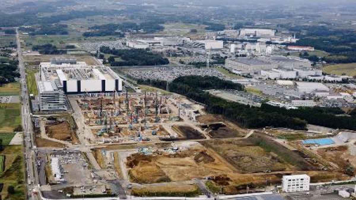
On October 16, 2026, Japan’s Ministry of Economy, Trade and Industry certified a change to the plan for JASM’s second Kumamoto fab. JASM — Japan Advanced Semiconductor Manufacturing, the Kumamoto joint venture TSMC owns about 86.5% of — will now build 3nm logic instead of 12nm and 6nm. The certification document sets output at 6,000 wafers a month in 12-inch equivalents, a project period running to December 2028, and first shipments in the fourth quarter of 2028. According to Kyodo, it is the first 3nm-class advanced semiconductor production in Japan; the filing is numbered 2023半経第003号-2.
Key points
- The certified document fixes six checkable numbers: 3nm logic, 6,000 wafers a month, a project period to December 2028, first shipments in Q4 2028, a 321,000 m² site and about 1,700 employees.
- The original certification of February 24, 2024 listed 12nm and 6nm chips, plus 40nm, at 48,000 wafers a month and 63,000 for the whole fab, with first shipments in Q4 2027. The change cuts planned capacity to one-eighth and pushes shipments back a year.
- METI revised JASM’s fab 1 plan the same day: products narrow from 22/28nm plus 12/16nm to 22/28nm, capacity falls from 55,000 to 45,000 wafers a month, and that project’s subsidy cap drops from ¥476bn to ¥409.5bn. Fab 2’s cap falls from ¥732bn to ¥645.15bn.
What happened
JASM is TSMC’s Kumamoto joint venture. TSMC holds about 86.5%, Sony Semiconductor Solutions about 6.0%, Denso about 5.5% and Toyota about 2%, according to the certification document. Fab 1 was certified on June 17, 2022, with first shipments scheduled for December 2024 on 22/28nm and 12/16nm logic. Fab 2 was certified on February 24, 2024 with a 12nm/6nm plan, a 40nm line alongside it, and 48,000 wafers a month.
The pivot came in February 2026, when TSMC chairman and CEO C.C. Wei met Prime Minister Sanae Takaichi and proposed moving fab 2 to 3nm. Taiwan’s Ministry of Economic Affairs approved the upgrade in March 2026, according to Tech Times. At TSMC’s October 15 earnings call the company said only that its second Japanese fab was on track for 2028 production on 3nm; our report on those results carries no capacity or subsidy figures. The numbers here come from METI’s October 16 certification.
The numbers in the filing
The revised certification runs four pages, and each figure can be checked against the original text. It lists the site as “Kumamoto Prefecture (specific location to be decided later),” which differs from the town-level address used by every news outlet; the construction site is in Kikuyo, but the filing does not go below prefecture level. The 321,000 m² site, 88,000 m² of building and roughly 1,700 employees are unchanged from the original certification, and FNN’s report says the site area and headcount did not move.
| Item | Original (2024-02-24) | Revised (2026-10-16) |
|---|---|---|
| Main products | 12nm and 6nm, plus 40nm | 3nm logic |
| Capacity | 48,000 wafers/month (63,000 whole fab) | 6,000 wafers/month |
| Project period | To December 2029 | To December 2028 |
| First shipments | Q4 2027 | Q4 2028 |
| Declared funding | $13.9bn ($12.2bn excluding 40nm) | $10.8bn |
The funding row needs its own note. The original filing reads “$13.9 billion scale ($12.2 billion excluding 40nm)”: $13.9 billion includes the 40nm line, $12.2 billion is the figure with it stripped out. The revised filing reads “$10.8 billion scale (facilities and equipment for which support measures are sought)” — only the portion applying for subsidies. The two parentheticals do different work. Nikkei writes that investment rose “from $12.2 billion to at least $15.7 billion,” starting from the ex-40nm number. Kensetsu News puts it at “over $15.7 billion, about ¥2.48 trillion.” FNN says the two fabs together come to “over $23 billion, over ¥3.5 trillion.” These are not the same quantity: $10.8 billion is the subsidized scope, $15.7 billion an estimate of the whole project.
Why the subsidy fell
Fab 2’s subsidy ceiling dropped from ¥732bn to ¥645.15bn, the easiest line in the certification to skip. METI’s index page lists a single maximum subsidy per project: the January archive of that page says ¥732bn, the current one says ¥645.15bn. On the same page fab 1’s ceiling fell from ¥476bn to ¥409.5bn, and the revised certification now listed under that entry is dated October 16. DIGITIMES reports the aid as “up to $4.1 billion”; ¥645.15bn converts to that at about ¥157 to the dollar (the conversion is mine).
A smaller subsidy alongside a larger investment is consistent once you separate the two quantities. Nikkei reports that METI has put a larger amount into its FY2027 budget request; Kensetsu News says the ministry is considering raising the figure because of the 3nm plan. ¥645.15bn is the current certified ceiling, not a final cap.
Divide with matched scopes and the cost of the change shows up. The original’s $12.2 billion excluding 40nm pairs with the 48,000 wafers a month that also exclude it: about $254 million per 1,000 monthly wafers. Use the $13.9 billion figure instead and the denominator has to be the 63,000-wafer whole-fab total, about $221 million. The revision asks $10.8 billion against 6,000, about $1.8 billion. On the first pairing, declared funding per unit of capacity rose about 7.1-fold; on the second, about 8.1-fold. That is this article’s arithmetic on the filings’ own numbers, not a METI statement. An EUV scanner costs about $200 million on its own (Tech Times’ figure), and a 3nm fab rebuilds its cleanroom and tool set to tighter specs.
What others say
Kyodo, republished by the Kumamoto Nichinichi Shimbun, has the fullest account: total investment of about $10.8bn, roughly ¥1.7 trillion; up to ¥645.15bn in METI support; initial output of 6,000 wafers a month; and capacity that will rise depending on support from the Japanese government. Note that Kyodo labels that $10.8bn the “total investment,” while METI’s own filing scopes it to the facilities seeking subsidies — same number, two different labels. Kumamoto governor Takashi Kimura said the decision would lead what he called a new creative reconstruction and that it was reassuring.
Nikkei leads with the change in figures: investment up from $12.2bn to at least $15.7bn, 6,000 wafers a month from December 2028, and ultimate capacity set by the size of government support. Kensetsu News adds TSMC’s statement, relayed rather than issued: specific production will be carried out in stages according to market demand, with Japanese government support as a precondition. I could not find a TSMC press release on the certification, so that relayed line is the only company comment available.
English coverage makes different trades. DIGITIMES carries only the aid ceiling. TaiwanPlus adds that fab 1 will shift to 22–28nm, which matches METI’s revised fab 1 filing, but its body also says the project was “initially planned at around $4.6 billion” — apparently the old subsidy figure read as an investment — so this article does not use it.
The counter-case comes from August’s earthquake coverage. A magnitude-7.1 quake hit Kumamoto on July 28, registering upper-5 on Japan’s intensity scale at Kikuyo. TSMC said at the time that “due to the relatively high seismic force of this earthquake,” inspections and calibrations would take additional time. The fab 2 construction site itself was unaffected and work resumed after extra safety checks, but Taiwan’s economy ministry warned the wider construction timeline could slip. EUV tools are acutely sensitive to vibration and require recalibration after a strong shock, and AI accelerator customers redesign chips on 18- to 24-month cycles, each generation needing fresh qualification.
Our take
Six thousand wafers a month is a small number against TSMC’s global 3nm output. It reads more like an entry ticket: Japan gets a legal 3nm production base, and capacity unlocks in stages as subsidies arrive. Three groups should care. Teams planning 2029 products that need leading-edge capacity outside Taiwan can put Kumamoto on the shortlist, but should not model supply on the 48,000-wafer figure. Equipment and materials suppliers in Kyushu face two different node generations in one campus, since fab 1 is narrowing to 22/28nm while fab 2 goes to 3nm, and should plan inventory separately. And anyone tracking Japanese industrial policy now has a filing that writes “subsidy for capacity” into clauses you can check.
Four limits. Output is an initial figure; Nikkei and Kyodo both say the final number depends on further subsidies, and the FY2027 budget is not settled. The timeline has already moved once. Earthquake risk has not gone away, and EUV calibration means one strong shock can cost weeks. Last, with fab 1 narrowed to 22/28nm, the 6nm and 12/16nm tier has disappeared from both filings’ product lists. I have not seen that point in any coverage; it falls out of reading the two certifications side by side. The 40nm line survives, listed under fab 1.
What to watch
Three dates are checkable. Whether the FY2027 budget request lifts fab 2’s subsidy ceiling above ¥645.15bn. Whether fab 1’s 22/28nm line starts operation in December 2026, per its revised filing. And whether first shipments land in Q4 2028. TSMC has not named Kumamoto’s 3nm customers, and with AI chips redesigned every 18 to 24 months, customer qualification will decide how fast those 6,000 wafers a month fill. Advanced logic is not the only tight link: memory shortages now run through 2028, and in-house accelerators like Microsoft’s Maia 300 compete for the same TSMC capacity.