Diamond Foundry says it made the first 200mm single-crystal diamond wafer
Diamond Foundry says it grew the first 200mm single-crystal diamond wafer, aimed at AI chip cooling; no third-party validation yet.
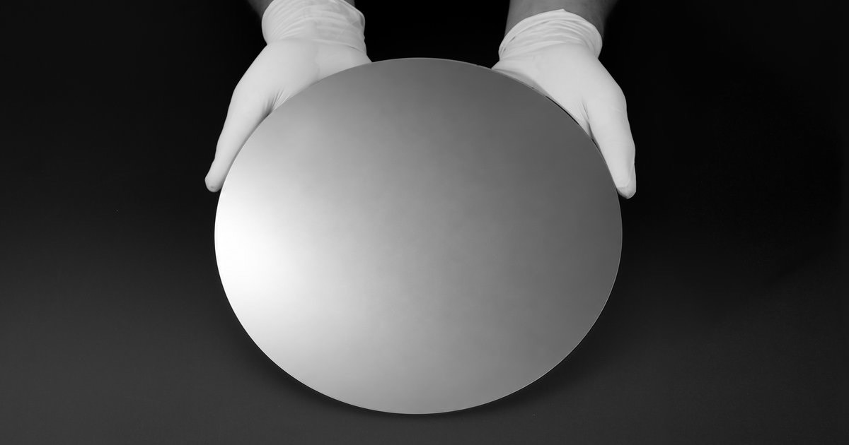
Diamond Foundry, the San Francisco company that made its name growing lab diamonds for jewelry, announced on November 5 that it has produced a 200mm single-crystal diamond wafer, which it calls the first of that diameter made of one continuous crystal. The wafer was shown as grown and unpolished. The company positions it as a substrate for AI chips: diamond conducts heat at roughly 2,200 W/(m·K) at room temperature, about 15 times silicon’s 149 W/(m·K), and hotspot cooling is one of the tightest physical limits on current AI processors.
Key points
- The November 5 announcement claims the world’s first 200mm single-crystal diamond wafer: one continuous crystal, not stitched from smaller pieces and not polycrystalline; the specimen shown was unpolished.
- Diamond’s room-temperature thermal conductivity is about 2,200 W/(m·K) — roughly 15 times silicon and 6 times 4H silicon carbide (348 W/(m·K)); the company’s play is moving chip cooling from packaging engineering down to the substrate material itself.
- Everything announced so far is the company’s own claim: no paper, no third-party characterization, no yield, price or shipping dates; the largest previously announced size was Diamond Foundry’s own 100mm wafer in October 2023.
Background
Diamond Foundry was founded in 2012 in San Francisco and built its first business on lab-grown diamonds for jewelry under the VRAI brand, pivoting toward semiconductor materials from 2023. Two pieces of background matter here. The company acquired Augsburg Diamond Technology (Audiatec) in 2022, bringing in Stefan Gsell and Martin Fischer, who had worked on large single-crystal growth for 25 years. And in Spain: its Trujillo fab started operations in January 2025 (five weeks ahead of schedule, per the company), and in November 2025 the company announced a $2.77 billion expansion with ingot-furnace construction underway; it says the site runs 24x7 on solar power with battery storage. The public milestone on this road came in October 2023, when Diamond Foundry announced a 100mm single-crystal diamond wafer weighing 110 carats, also billed as a world first. On the industry side, Japan’s Orbray (formerly Adamant Namiki) and Saga University produced a 2-inch (about 55mm) single-crystal wafer in 2021 and announced a mass-production method in April 2022, using heteroepitaxial step-flow growth on sapphire with nitrogen kept under 3 ppb. Single-crystal diamond had stayed near the inch scale for years — that is the backdrop against which a 200mm claim lands.
The facts
The announcement itself carries few checkable specifics: the wafer is 200mm across, and the company stresses it is one continuous crystal — not pieces joined together, not a polycrystalline aggregate — displayed as grown and unpolished. CEO Martin Roscheisen said in the announcement: “This is one of those milestones that once seemed almost impossible,” adding that hundreds of engineers, scientists and technicians contributed. On what comes next, the announcement quotes Roscheisen saying the 200mm result “makes D300mm predictable as well,” with no timeline attached.
The material numbers can be checked independently. Wikipedia’s materials entry puts natural type-IIa diamond at roughly 2,200 W/(m·K) at room temperature, with isotopically enriched ¹²C synthetic diamond reaching 3,320 W/(m·K) — about 15x silicon and 6x 4H silicon carbide on the same reference values. The company’s marketing multiples, such as “up to 10x power,” come without published test conditions; this piece uses the encyclopedia figures.
| Material | Thermal conductivity, room temp (W/(m·K)) | Note |
|---|---|---|
| Diamond (natural type IIa) | ~2,200 | ¹²C-enriched synthetic samples reach 3,320 |
| Copper | 401 | Traditional heatsink baseline |
| Silicon carbide (4H) | 348 | Mainstream power-electronics substrate |
| Silicon | 149 | Standard chip wafer |
On its product page the company claims diamond substrates let AI chips run at “up to 10x” power and “up to 10x” lifetime, “up to 100x” cooling capacity, and “up to 7x” FLOPS/kWh in 3D packaging — none of these figures has third-party test data behind it. The announcement lists semiconductor substrates, power electronics, optics and quantum devices as target uses.
What others say
As of publication, the story has circulated mainly through outlets such as MyDrivers relaying the company’s announcement; Diamond Foundry has not published a paper, independent lab characterization or customer validation, so the “world’s first” framing cannot be verified externally. Two kinds of independent reference do exist. One is the materials science itself: diamond’s thermal conductivity tops every known solid while it stays an electrical insulator with high mechanical strength — settled textbook territory. The other is industry history: Orbray and Saga University’s 2-inch wafer line used heteroepitaxy, and after announcing mass production in 2022 it never scaled widely. When Diamond Foundry’s 100mm announcement was posted to Hacker News in January 2024, it drew 5 points and zero comments; the 200mm announcement is about two days old and no independent discussion thread has appeared yet. The two approaches differ, but they point to the same conclusion: the barrier to wafer-scale single-crystal diamond is engineering scale-up, not the existence of the material.
Our take
Moving heat from packaging engineering down to the substrate material is a direction that holds up on its own merits. AI chip power density keeps climbing: Microsoft’s Maia 300 sells on tokens per megawatt, Nvidia’s DSX POD packs whole racks into a shipping container while racing the same thermal limits, and a diamond substrate, if it works, pays off at the material level. Power electronics points the same way — the US Commerce Department issued research awards for power semiconductors in October, a sign that substrate materials themselves are where bets are placed after silicon carbide. But read this announcement with three caveats. It is a company claim with no paper and no third-party characterization. The specimen shown is unpolished as-grown material — polished, defect-controlled, bondable chip-grade substrates still sit several steps away, along with cost. And yield and pricing went unmentioned; “available in volume” is currently one sentence on a product page. Reading it as a signal about where materials scaling is heading is reasonable. Reading it as capacity you can buy soon is not.
What to watch
Three markers are worth following. First, a paper or independent characterization — if a 200mm single crystal is real, academic groups usually follow with X-ray diffraction and defect imaging. Second, the 300mm roadmap, which the announcement calls predictable without giving a date. Third, when the product page lists real specifications and prices behind its buy buttons. Orbray’s 2-inch wafer took about seven months from result to a mass-production claim and never scaled widely — the history of wafer-scale diamond has issued this warning once already.